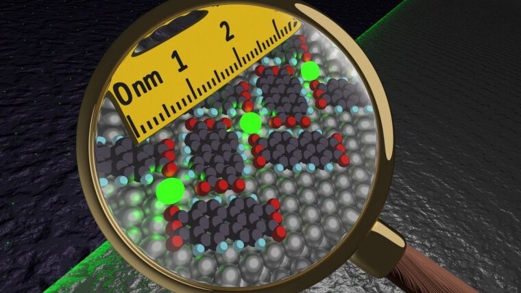
We are active in the fundamental research in the field of molecular electronics. In this context, we comprehensively investigate the structural and physical properties of ultrathin highly ordered molecular layers on different single-crystalline substrates in order to lay the foundations for future organic-based (opto-)electronic devices.
Are you interested in a Bachelor's, Master's or doctoral thesis? Please contact Prof. Dr. Torsten Fritz and ask for an appointment. Together with you we will find a topic which best suits your skills, and which is integrated in our cutting-edge research. You are encouraged to come by and get to know our friendly colleagues and visit our state-of-the-art labs.
Main Topics
- Organic molecular beam epitaxy (OMBE)
- Modern 2D materials "graphene and beyond" (h-BN, BlueP, MoS2, ...)
- Organic-inorganic and organic-organic heterostructures
- Structural characterization of highly ordered molecular layers on metal, semiconductor and insulator surfaces using scanning probe microscopies (STM, AFM, STHM) at 1.1 K and electron diffraction methods (LEED, RHEED)
- Optical in situ spectroscopy of ultrathin films in absorption (DRS) and emission (PL)
- Photoelectron spectroscopy (ARUPS, XPS), Measurement of band structures
- Photoelectron momentum maps (PMM), also called orbital tomography
- Auger electron spectroscopy (AES) for the measurement of depth profiles
- Determination of the epitaxy type
- Electronic interface effects (electronic coupling, hybridization, charge transfer
Equipment and Methods
-
SPECS Joule-Thomson STM/AFM
Experimental Methods
- STM, STHM, STS, and AFM
- MCP-LEED
- DRS
- QMS
Features
- Temperatures in the STM/AFM down to approx. 1 K
- Temperatures for MCP-LEED and DRS down to approx. 20 K
- Magnetic field in the STM/AFM up to 3 T
- 4-probe measurements
- Crucibles for organic molecules
- Doping with alkali metals and alkaline earth metals
- Argon sputter gun and electron bombardment heating
-
SPECS Surface Analysis System
Experimental Methods
- XPS (ESCA), UPS, ARUPS
- MCP-LEED
- AES
- DRS
- QMS
Features
- Temperatures for XPS, UPS, and ARUPS down to approx. 20 K
- Monochromatized UV light source
- Crucibles for organic molecules
- Doping with alkali metals and alkaline earth metals
- Argon sputter gun and electron bombardment heating
-
UNISPEC Surface Analysis System
Experimental Methods
- XPS (ESCA), UPS, ARUPS
- RHEED
- AES
Features
- UV and X-ray light sources
- UHV preparation chamber with crucibles
- Argon sputter gun and electron bombardment heating
- Sample preparation at high temperatures of up to 1700 K
- Growth of 2D-materials such as h-BN and BlueP
-
OMBE-Barrel
Experimental Methods
- MCP-LEED
- AES
- DRS
- QMS
Features
- Crucibles for organic molecules
- Doping with alkali metals and alkaline earth metals
- Argon sputter gun and electron bombardment heating
-
OMBE-Sphere
Experimental Methods
- LEED
- QMS
- STM (@ 300 K)
Features
- Crucibles for organic molecules
- Argon sputter gun and electron bombardment heating
-
Auger Analysis System
Experimental Methods
- AES
- Depth profiling
Features
- Electron gun and ion gun
- CMA electron energy analyzer
- Analysis of material composition
-
Temperature Gradient Sublimation
Features
- Purification of sublimable organic substances in high vacuum
- 3-zone furnace
- Computer-controlled heating traces
- Storage of sublimation protocols for various substances
-
CVD
Features
- Chemical vapor deposition
- Growth of epitaxial graphene
- Growth of carbon nanotubes
- High-temperature hydrogen etching of SiC
- RF generator
-
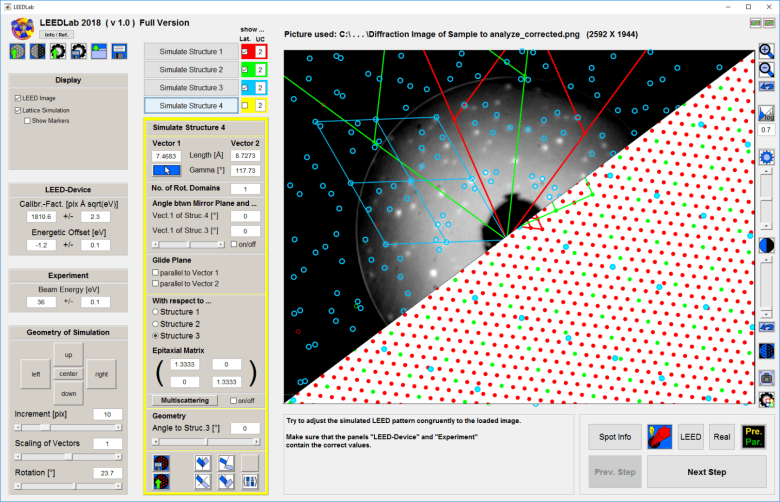
Software LEEDCal and LEEDLab
Learn moreExternal linkScreeshot LEEDLab
Screenshot: Falko SojkaLEEDCal
- Analysis of systematic distortions (radial, asymmetric) specific to your LEED device based on a reference measurement
- Provision of a correction rule for all your LEED images
- Application of the correction rule feasible in batch processing mode
Download LEEDCal 2013External link and LEEDCal_corr 2013External link
MATLAB Runtime (R2013a (8.1)) 64-bitExternal link is additionally required for execution
LEEDLab
- Geometric simulation of diffraction patterns of complex surface structures
- Direct comparison with your own LEED images
- Viewing in real and reciprocal space feasible (fast changeover)
- Objective determination of lattice parameters and epitaxial relations
Download LEEDLab 2018External link
MATLAB Runtime (R2013a (8.1)) 64-bitExternal link is additionally required for execution
